Discussion summary

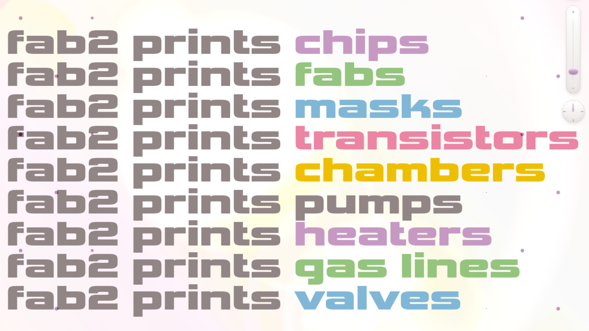
Jim Keller's startup is developing a factory for small chip fabs aimed at democratizing chip manufacturing. Discussions highlight potential, technical feasibility, and economic challenges of small-scale fabs.

What the discussion says

  • Small fabs could enable rapid prototyping and local manufacturing.
  • Electron-beam lithography allows very small transistors but is costly.
  • Small fabs are suitable mainly for prototyping and low-volume runs.
A small fab using electron-beam lithography can do everything TSMC can, but it's more economical.
adrian_b
Their website is quite difficult to navigate, which is a concern.
syntaxing

Comments

Hacker News

Great! Hopefully we can get 10 year behind technology from small fabs. There's so much you can do with a laptop from 2016

by vatsachak

Global Foundries has lots of fabs with 10 year old+ processes....

by phonon

With electron-beam lithography you can build transistors with gate lengths down to 1 to 3 nanometers.

by pulse7

No, you misunderstood.

A small fab that uses electron-beam lithography can do everything that TSMC can do, and in a much simpler way.

Its problems are not technical, but economical.

The costs of producing chips are much lower than for TSMC, but the production rate is also orders of magnitude lower.

So they can be used only to produce prototypes or devices for niche applications, where the small quantities needed would never allow them to be produced at a big fab.

On the other hand, if such small fabs could be themselves mass produced, so that their cost could become low enough, then using a great number of such small fabs could satisfy the requirements in semiconductor devices and ICs of most not too big countries, and this style of production would be greatly preferable to what exists today as the end point of a long chain of acquisitions and mergers, that has resulted in a handful of SOTA manufacturers in the entire world.

Ideally, there would still exist big fabless IC design companies, like Intel, AMD or NVIDIA, but they would design for a standardized CMOS fabrication process, not for a proprietary process with secret design rules, like those of TSMC.

Then such designs would be licensed for production in distributed small fabs. Only such a system would remove the dependence of the entire world on a quasi-monopolistic system of production, where the destruction of a single fab could cripple most of the world.

by adrian_b

How could would ut be that your company or university or even at home has its own chip machine. Design your 5b transistor chip and bake and process it the same day. Doable I would say.

by holoduke

This is a great idea and hope it works out, especially on shoring chips back here in the states. That being said, their website is absolutely atrocious. One of the very few sites I got motion sickness from scrolling.

[1] https://fab2.com/

by syntaxing

It even manages to lag on my one year old flagship phone! Impressive! :)

by Melonai

Is this an ASML competitor?

by eikenberry

No, quoting the article:

> only really suits prototyping and low-volume runs rather than high-volume production at commercial foundries

by re-thc

This is "we fit on small FPGA but dont want to ship cheap commodity off the shelf hardware for some bizarre reason while cant even afford structured ASIC (you only pay for metal layer masks)" competitor maybe.

Unless they offer some amazing analog capabilities.

by rasz

One of the most interesting technologies that is not about LLMs/AIs.

by d_silin

I would've liked to read more about what they're doing, but their website fab2.com is unhelpful. Very little info, presented in pointless swirling animations that hijack your scroll action.

by ripe

Yes, the web site is all effects, no content. It's like an old Flash site.

E-beam machines work fine for prototyping. People have been doing that since the 1970s. But they're slow. It's a prototyping technology. The sort of thing that "3D print everything" people like. E-beam machines with many beams have been mentioned, but never seemed to be worth it.

There are companies which offer E-beam IC fab as a service. Some cater to DoD and the intelligence community.[2] (That's for when you really can't trust your supply chain and want your own ICs fabbed.) Others are more commercial, but are in China.[3]

They claim to be building all the machines needed for a fab. But they don't have a list, or pictures. There's a used market in that gear, and no reason to build it all yourself.

It's not a fundamentally bad idea, but the hype is strong here.

[1] https://www.machinio.com/semiconductors

[2] https://www.hrl.com/laboratories/mtl

[3] https://en.omedasemi.com/electron_beam_lithography.html

by Animats

> ... chip architect Jim Keller and DIY fabrication pioneer Sam Zeloof, has rebranded as Fab2 and moved its operations to Texas

> Fab2 now operates three sites: a 120,000 square foot facility in Austin serves as the new headquarters for research and production, a 30,000 square foot site in Lockhart houses the "fab fab" itself, and the original 25,000 square foot "garage fab" remains in San Francisco.

> Fab2 said it shifted its hiring focus to Texas after four years in California

Is California not what it used to be for startups? (I'm not saying Texas doesn't have an history of tech startups: it had the likes of Texas Instruments and many others in the early days)

by TacticalCoder

Applied for a job, but their recruiter was trash. Still, hope it works out for the company.

by jtullos

I don't get it. How is Jim Keller running a brand new, hard tech startup while being CEO of Tenstorrent at the same time?

by ipsum2

So Elon Musk can be the CEO of multiple companies but Jim Keller can't be CEO of two quickly growing startups?

by wyre

There are rumors Qualcomm is going to buy Tenstorrent.

by bhewes

Chuck Norris will pass his torch to Jim Keller.

Jim won't have a say in the matter.

by CoastalCoder

I’m a semiconductor expert and without seeing the details, this seems like yet another smoke and mirrors wunderkind startup that will disperse once practical considerations are made. As far as I know, Mr. Zeloof has not made any fundamental advancements in any steps in manufacturing.

by georgeburdell

The article mentions, but doesn't explicitly state, that they're going to be using electron beam lithography. Makes sense for their low volume and/or prototype fab goal, but I'm curious how well that would work for prototyping to fab at high volume with the likes of TSMC or Intel.

I would assume that re-targeting a design to a different fab's process would change enough about it that you might as well just do verification in simulation rather than sidetrack through Fab2.

by sq_

I think this might make a lot of sense in modern warfare scenarios: We're seeing in Ukraine that being able to produce weapons such as drones in very small production facilities using 3D printers and 'simple' technology makes it very hard for an adversary to shut down said production.

The more components can be produced in such a way, the better. Chips currently are quite an exception to that.

by dinfinity

Featured on the frontpage four years ago: https://news.ycombinator.com/item?id=30043719 (22-year-old builds chips in his parents’ garage | 525 | Jan 23, 2022 | 347 comments)

I still recall being amazed reading and seeing it for the first time, and I have been eagerly awaiting to see what he been up to since starting Atomic Semi.

by embedding-shape

Join the discussion

Write your take first — we'll ask for email only when you're ready to publish.

  • Hacker News
  • Great! Hopefully we can get 10 year behind technology from small fabs. There's so much you can do with a laptop from 2016
    by vatsachak
  • Global Foundries has lots of fabs with 10 year old+ processes....
    by phonon
  • With electron-beam lithography you can build transistors with gate lengths down to 1 to 3 nanometers.
    by pulse7
  • No, you misunderstood.

    A small fab that uses electron-beam lithography can do everything that TSMC can do, and in a much simpler way.

    Its problems are not technical, but economical.

    The costs of producing chips are much lower than for TSMC, but the production rate is also orders of magnitude lower.

    So they can be used only to produce prototypes or devices for niche applications, where the small quantities needed would never allow them to be produced at a big fab.

    On the other hand, if such small fabs could be themselves mass produced, so that their cost could become low enough, then using a great number of such small fabs could satisfy the requirements in semiconductor devices and ICs of most not too big countries, and this style of production would be greatly preferable to what exists today as the end point of a long chain of acquisitions and mergers, that has resulted in a handful of SOTA manufacturers in the entire world.

    Ideally, there would still exist big fabless IC design companies, like Intel, AMD or NVIDIA, but they would design for a standardized CMOS fabrication process, not for a proprietary process with secret design rules, like those of TSMC.

    Then such designs would be licensed for production in distributed small fabs. Only such a system would remove the dependence of the entire world on a quasi-monopolistic system of production, where the destruction of a single fab could cripple most of the world.

    by adrian_b
  • How could would ut be that your company or university or even at home has its own chip machine. Design your 5b transistor chip and bake and process it the same day. Doable I would say.
    by holoduke
  • This is a great idea and hope it works out, especially on shoring chips back here in the states. That being said, their website is absolutely atrocious. One of the very few sites I got motion sickness from scrolling.

    [1] https://fab2.com/

    by syntaxing
  • It even manages to lag on my one year old flagship phone! Impressive! :)
    by Melonai
  • Is this an ASML competitor?
    by eikenberry
  • No, quoting the article:

    > only really suits prototyping and low-volume runs rather than high-volume production at commercial foundries

    by re-thc
  • This is "we fit on small FPGA but dont want to ship cheap commodity off the shelf hardware for some bizarre reason while cant even afford structured ASIC (you only pay for metal layer masks)" competitor maybe.

    Unless they offer some amazing analog capabilities.

    by rasz
  • One of the most interesting technologies that is not about LLMs/AIs.
    by d_silin
  • I would've liked to read more about what they're doing, but their website fab2.com is unhelpful. Very little info, presented in pointless swirling animations that hijack your scroll action.
    by ripe
  • Yes, the web site is all effects, no content. It's like an old Flash site.

    E-beam machines work fine for prototyping. People have been doing that since the 1970s. But they're slow. It's a prototyping technology. The sort of thing that "3D print everything" people like. E-beam machines with many beams have been mentioned, but never seemed to be worth it.

    There are companies which offer E-beam IC fab as a service. Some cater to DoD and the intelligence community.[2] (That's for when you really can't trust your supply chain and want your own ICs fabbed.) Others are more commercial, but are in China.[3]

    They claim to be building all the machines needed for a fab. But they don't have a list, or pictures. There's a used market in that gear, and no reason to build it all yourself.

    It's not a fundamentally bad idea, but the hype is strong here.

    [1] https://www.machinio.com/semiconductors

    [2] https://www.hrl.com/laboratories/mtl

    [3] https://en.omedasemi.com/electron_beam_lithography.html

    by Animats
  • > ... chip architect Jim Keller and DIY fabrication pioneer Sam Zeloof, has rebranded as Fab2 and moved its operations to Texas

    > Fab2 now operates three sites: a 120,000 square foot facility in Austin serves as the new headquarters for research and production, a 30,000 square foot site in Lockhart houses the "fab fab" itself, and the original 25,000 square foot "garage fab" remains in San Francisco.

    > Fab2 said it shifted its hiring focus to Texas after four years in California

    Is California not what it used to be for startups? (I'm not saying Texas doesn't have an history of tech startups: it had the likes of Texas Instruments and many others in the early days)

    by TacticalCoder
  • I saw some innovative nuclear projects are also building in Lockhart https://oklo.com/isotopes/texas/default.aspx
    by stogot
  • Applied for a job, but their recruiter was trash. Still, hope it works out for the company.
    by jtullos
  • I don't get it. How is Jim Keller running a brand new, hard tech startup while being CEO of Tenstorrent at the same time?
    by ipsum2
  • So Elon Musk can be the CEO of multiple companies but Jim Keller can't be CEO of two quickly growing startups?
    by wyre
  • There are rumors Qualcomm is going to buy Tenstorrent.
    by bhewes
  • Chuck Norris will pass his torch to Jim Keller.

    Jim won't have a say in the matter.

    by CoastalCoder
  • I’m a semiconductor expert and without seeing the details, this seems like yet another smoke and mirrors wunderkind startup that will disperse once practical considerations are made. As far as I know, Mr. Zeloof has not made any fundamental advancements in any steps in manufacturing.
    by georgeburdell
  • The article mentions, but doesn't explicitly state, that they're going to be using electron beam lithography. Makes sense for their low volume and/or prototype fab goal, but I'm curious how well that would work for prototyping to fab at high volume with the likes of TSMC or Intel.

    I would assume that re-targeting a design to a different fab's process would change enough about it that you might as well just do verification in simulation rather than sidetrack through Fab2.

    by sq_
  • I think this might make a lot of sense in modern warfare scenarios: We're seeing in Ukraine that being able to produce weapons such as drones in very small production facilities using 3D printers and 'simple' technology makes it very hard for an adversary to shut down said production.

    The more components can be produced in such a way, the better. Chips currently are quite an exception to that.

    by dinfinity
  • That's the one that Sam Zeloof is working on, "having lithographically microfabricated various chips in his garage as early as the age of 17"

    https://en.wikipedia.org/wiki/Sam_Zeloof

    by WithinReason
  • Featured on the frontpage four years ago: https://news.ycombinator.com/item?id=30043719 (22-year-old builds chips in his parents’ garage | 525 | Jan 23, 2022 | 347 comments)

    I still recall being amazed reading and seeing it for the first time, and I have been eagerly awaiting to see what he been up to since starting Atomic Semi.

    by embedding-shape

Related stories