Join the discussion

Write your take first — we'll ask for email only when you're ready to publish.

  • Hacker News
  • This is somewhat orthogonal to the article, but the whole bubble on AI data centers seems to presume that the need for compute is so massive that it far exceeds the expected optimizations we would expect with at scale inference (PIM, ASICs, etc). I would expect that there is a set of optimizations like this one (or variations) that would someone negate the buildout. But it's not really discussed.
  • It's not just inference, some things done in data centers like simulations, testing, are complementary to inference.

    And in these types of hardware, the time between a successful prototype and a fully deployed product is pretty long. Maybe they count on that to know when to stop?

  • Jevons Paradox shows that increasing efficiency can increase demand for a product by making it cost effective for more uses.
  • There's been a ton of optimizations already, it hasn't remotely reduced demand even temporarily. More efficiency just makes the compute have even higher ROI per $ and watt spent.
  • “ Each PIM block only has fast access to its locally attached DRAM bank. All other input data has to be brought in through the DRAM chip’s comparatively constrained external interface. PIM blocks can’t directly exchange data with each other, so the host has to move data using regular DRAM reads and writes if one PIM block needs to use results generated by another.”

    So how big are these banks? If you can’t fit the weights of a layer into one bank then presumably you lose a lot of the speed gains.

  • For GEMV you lose nothing.

    The reason is quite simple. You can split the matrix along both dimensions so you just tile it into 64x64 or whatever fits into the bank and just fill it up. The biggest problem is load balancing the tiles across all banks for maximum parallelism.

    For GEMM I believe there is no point in doing PIM, you are better off with a GPU or NPU.

  • Not necessarily. If your weights have to go across 2 banks, you just have to split and transfer the input and output vectors, which are much smaller.
  • In memory compute has been in talks since LLMs took up. I remember few flocks were trying to get RISC V cores in the memory like these papers

    https://arxiv.org/abs/2602.01827

  • It has been a prominent "next major shift" idea in computer architecture since the 90s, to deal with the memory wall. Eg David Patterson advocating it in the 1990 and 1997 articles. or CRAM [1].

    [1] https://www.eecg.toronto.edu/~stumm/Theses/Elliott-PhD98.pdf

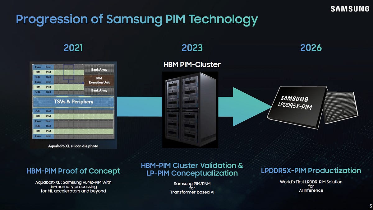
  • Interesting that Samsung still pursues PIM. IIRC they had a paper in ISCA21 or 22 where they showed HBM2 module with PIM, which back then impressed me quite a lot.

    That being said, I am not sure what’s the killer application for this technology, and without such application adoption is unlikely.

  • > That being said, I am not sure what's the killer application for this technology...

    Build it, and they will come ;)

  • The idea is this:

    You have an eight socket server with 96 memory slots, you add 96x PIM memories into the server (optimistic), load all the LLM parameters or KV cache in RAM and exclusively let it perform GEMV and let it rip.

    614 GB/s x 96 = 58,944 GB/s.

    Alternatively, the memory is used for embedded inference tasks. You can now upgrade from the limited single or two digit MB SRAM accelerators to reasonably fast single digit gigabyte models. Without MoE you could reach 100 tokens per second with an 8B fp8 model on a single channel. With MoE you might break 500 tokens per second.

  • As I understand it, the killer app is llms. You could run MACs directly in RAM, offloading a lot of work from CPU and cutting down on insane (external) memory bandwidth required.

    Imagine (this is a fantasy pitch but potentially achievable for some use cases) wanting to run a larger llm and all you have to do is buy more RAM so it fits.

  • Might as well just go whole hog and change the entire computer architecture, then. A lot of the arguments against this change boil down to computers and software code don’t work well with this today.
  • So instead of putting more cache on the cpu you just put the cpu on the cache.
  • Sort of, but the cache architecture is replaced with memory architecture. But you could look at it either way.
  • So you basically dispose of cache for the memory region used? I wonder what the offsets of the cache misses is going to be in practice (the article addresses it but there is no solution/impact given by samsung).
  • I guess you also get very high bandwidth that way? I‘m not sure that would come for free though.
  • if your working set fits in cache PIM is irrelevant
  • > So you basically dispose of cache for the memory region used? I wonder what the offsets of the cache misses is going to be in practice (the article addresses it but there is no solution/impact given by samsung).

    This is a temporary issue. JEDEC's LPDDR6-PIM is going to add defined commands for Processing-in-Memory operations. Once there are standardised commands, it will be possible for the CPU vendors to make the CPU cache aware of what is happening.

    Of course, that doesn't solve it for this generation of the technology. But I think this generation is more of a demo for early adopters to gain experience with it. It will likely take a few years for all these issues to be solved, but there is no principled reason why they can't be.

  • What I find amusing about moving compute to a RAM bank is it _almost_ resembles where we were with ISA-based extended RAM back in the 1980's. Some cards featured a CPU that took over the whole system and/or functioned like an upgrade. Others were a "computer on a card" that provided other features. I think this goes to show how cyclic tech can be. So, something like Samsung's invention here might have gained traction, as overcoming the slow PC ISA bus would have been a huge accelerator, kind of like where we are now.
  • Maybe we can connect multiple Samsung RAM sticks to a grid and call it RAMsputer.
  • Whilst processing in memory is clearly the future, I am unconvinced by this implementation.

    Matrix multiplication involves getting every entry of the input and output matrices to be at the same multiplier at the same time. (Ie. N^2).

    To do that, a lot of data movement needs to happen. Movement is the main thing - the multiplication and addition is a sideshow as far as energy and silicon space is concerned. You need a 'around the chip' ring shift register to pass every element of one matrix past every element of the other.

  • Not if you have duplicates of rows on the first matrix, which can be done very efficiently if you build specialized hardware. Then its all just forward in parallel.
  • you're absolutely correct that pim without a real discussion about how that works in a broader communications context is kind of useless.

    what I find strange is the adoption of a standard synchronous dram interface. that's a horrible left over piece of architecture that severely constrains the applicability of this device. control flow on the dram side can't initiate any transactions on its own, or respond after work has been done - its like usb, except with a hard limit on the response.

    that severely limits the utility of the in-memory processors to doing things like encryption and compression - but even then those impose delays that effect the consistency model across that interface.

  • > Whilst processing in memory is clearly the future

    How clear is that? The idea has been around for about 60 years, and many attempts made by people who thought the same thing. Maybe this time it'll be the future.

  • People have been calling processing-in-memory "the future" since at least the 1980s. No one has been able to reduce the concept to a useful implementation but there is a long history of failed attempts.

    At this point processing-in-memory has taken on the aura of fusion power.

  • Given how important matrix multiplication with a huge number of fixed parameters is becoming, there is an enormous incentive to design much more efficient architectures where this very simple compute is colocated with memory. Inference cost would come down a lot.
  • "Movement is the main thing" is precisely why pursuing compute-in-RAM makes some sort of sense to begin with. But DRAM fabrication processes are quite specialized and do not perform well with pure compute logic. The overall profile of this thing will arguably be similar to a rather weak NPU, though with much better memory bandwidth - one key limitation, as with NPUs, will be the bespoke programming model and lack of support for the latest compressed/quantized number formats, which heavily limits the usefulness of being able to access memory directly. GPUs, even weak iGPUs, can dequantize/pad parameters on the fly which adds a lot of flexibility - and expose standard, well understood compute capabilities via CUDA, Metal or Vulkan. This is not quite comparable unfortunately.
  • I saw them present a similar concept at Hot Chips in 2020 or 2021. It's still a cool idea, however people should remember that there are like 20 of these exotic accelerators designs pitched at trade shows every year that go nowhere.